Materials
The classification of materials into metal, semi metal, semiconductors and insulators is usually done based on their band structure as shown in Fig. 1
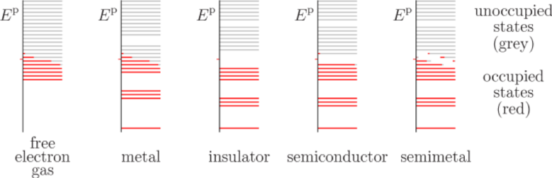
Figure 1. Sketch of electron energy spectra in solids at a nonzero temperature.
Taken from quantum mechanics for engineers. http://www.eng.fsu.edu/~dommelen/quantum/style_a/pboxbt.html
One can see that in metals the upper occupied level is within a continuum while in insulator there is a large energetic gap between the top occupied level which is completely filled and the next level. In semiconductors (intrinsic) the finite temperature is enough to allow electrons to overcome this gap and partially filled the next level. Because there are now two unfilled bands the original “insulator” has turned into a “semiconductor”.
The unique properties of a semiconductor are:
The concept of band structure is derived from the arrangement of the elements in the lattice that gives rise to delocalised electronic states. As a result, it is therefore highly sensitive to defects (such as impurities and crystallite boundaries). Fabrication of high-quality crystal, mainly silicon, is very expensive and is a primary obstacle for large area photovoltaics and circuitry. The costs are even higher when luminescent semiconductor crystals for LEDs are considered. An elegant solution is to use materials with intrinsic semiconductor behavior that is not related to their spatial configuration. An example of such class of materials are molecular semiconductors. In this class the “semiconducting behavior” is mostly inherent to the molecule it self with smaller effects due to three-dimensional structure. A huge advantage of such class of materials is the ability to engineer their electrical and optical properties by synthetic chemistry. As a result, this field is dominated by organic (carbon based) molecules due to the superb flexibility of organic chemistry.
From atomic orbits to conjugation
The solution of the Schrödinger equation for an atom results in the concept of shells that are filled in accordance to the rule outlines in Fig. 2.
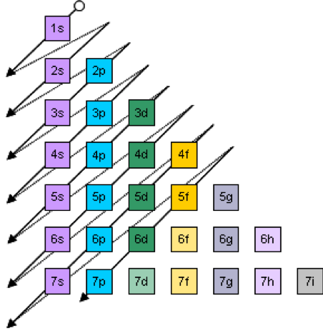
Figure 2. Order of filling of atomic sub shells. Each shell can be occupied by 2(n2) electrons (n goes from 1 to 7) and each sub-shell has 2, 6, 10, 14.. electrons for the s, p, d, f sub-shells, respectively.
Each atomic orbital has its own three-dimensional representation based on its angular momentum as depicted in Fig. 3.
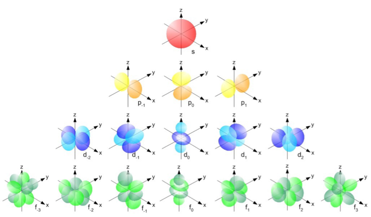
Figure 3.Three dimensional representation of electron probabilities for atomic orbitals.
Taken from University of California, David ChemWiki Page. http://chemwiki.ucdavis.edu/
Moving from an atom to a molecule there is a change in the orbitals due to the interaction between the atoms. The number of molecular orbits is identical to the number of atomic orbitals used to create them. Molecular orbitals are filled in accordance to their energy.
Sp2 hybridization and the conjugation of carbon-carbo- bonds
As an example of the process of molecular orbit formation let us observe the 1,3 Butadiene molecule. In Fig 4. it is shown that level 2 of carbon is the outermost shell. This level is consisted of a filled 2s-level and partially filled 2p-level (4(a)). When the 1,3 Butadiene molecule is formed the three-dimensional configuration of the bonds is called sp2 hybridization (Fig. 4(b)) where the original atomic orbitals are mixed to create three new orbitals in the plane and one unchanged orbital that is perpendicular to it. This result of the hybridization and the formation of the molecule is that the three paired sp2 atomic orbitals (two with hydrogen and one with the adjacent carbon atom, Fig 4. (c)) has a lower energy then the unpaired pz orbital (Fig 4. (d)).
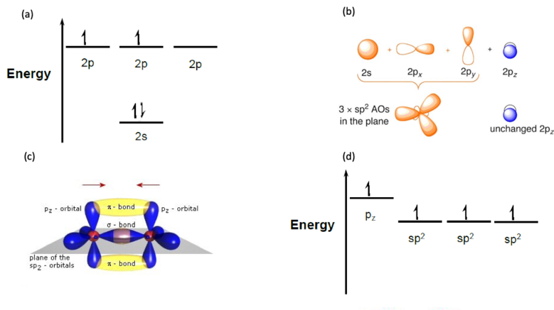
The sp2 bonds are called σ bonds and have electrons that are localized to the bond. In contrast the two pz orbits form a weaker, delocalized bond called π bond. These bonds can extend over many carbon atoms, a process known as conjugation. The length of the conjugation is defined by the atoms and the three-dimensional configuration of the molecule.
The energy diagram of the possible pz electrons for the individual atoms and for the molecules is shown in Fig. 5.
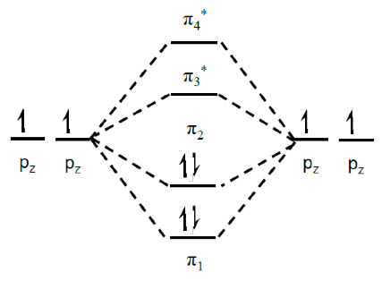
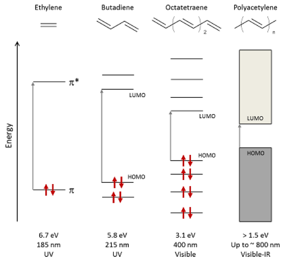
In this case, π2 is the Highest Occupied Molecular Orbital (HOMO) energy level and π3* is the Lowest unoccupied Molecular Orbital (LUMO) energy level. The splitting between the bonding, π, states and the antibonding, π* state is the equivalent to the energy gap in conventional semiconductors. As the number of molecules increases inner distance between the HOMO and LUMO decreases as can be seen in Fig. 6.
Taken from www.oe.phy.cam.ac.uk/research/materials/osemiconductors.html
Organic vs inorganic semiconductors
Sp2 Commonly used small molecules and polymeric materials

Figure 7. Hole-transporting (a) and electron transporting (b) commonly used organic small molecules (Mishra, A. Bäuerle, P. Angew. Chem. Int. Ed. 2012 51 2020. . Hole-transporting (c) and electron transporting (d) commonly used polymers (Boudouris, B. W . Cuee. Opi. Chem. Eng. 2013 2 294.